
Understanding the Role of a Silicon Carbide Coating Wafer Holder in Advanced Semiconductor Processing
In high-temperature semiconductor processes such as epitaxial deposition, etching, and diffusion, the component that physically supports the wafer is just as critical as the process chemistry itself. A silicon carbide coating wafer holder must withstand aggressive plasma, corrosive gases, and thermal cycling without shedding particles or releasing metallic contaminants into the process chamber. Traditional materials like quartz or standard graphite tend to degrade quickly in these aggressive chemical or plasma environments, resulting in outgassing, particle shedding, and batch contamination that directly compromises wafer yield and increases operating costs. This is the exact pain point that Wuyi Tianyao New Material Technology Co., Ltd., operating under the brand VeTek Semiconductor (also known as Veteksemicon / VETEK), has built its product portfolio around since its founding in 2016 in Wuyi City, Jinhua, Zhejiang Province, China.
Core Technical Foundation Behind VeTek's Wafer Holder Products
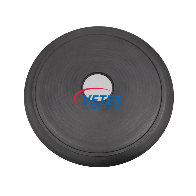
VeTek Semiconductor's CVD SiC Coated Wafer Susceptor is engineered specifically for epitaxial deposition of gallium nitride (GaN), silicon carbide (SiC), and silicon-based layers. The susceptor holds 6", 8", and 12" wafers securely during chemical vapor deposition while promoting thermal uniformity to minimize thermal stress on the substrate. Its defining feature is contamination control: an ultra-high purity level of ≤ 100ppb (ICP-E10 certified) that prevents metallic outgassing, ensuring clean epitaxial layer growth up to 1600°C.
This performance is not accidental — it stems from the company's vertically integrated manufacturing capabilities, which cover prefabrication, hot pressing, purification, machining, and chemical vapor deposition, combined with a dimensional capability exceeding 700mm. This allows for rapid customization and significantly shortened production cycles compared to traditional processes. On the metrics side, the company's CVD SiC purity reaches 99.99995% (impurity level below 5ppm, harmful metals below 1ppm), and machining precision reaches up to 3μm, with maximum processing dimensions of 1200mm × 1500mm. Solid CVD SiC used in related holder-type components achieves a density of 3.2g/cm³, a growth rate of ≥ 0.15mm/h, and a resistivity range of 10^-2 to 10^4 Ω·cm.
Beyond the Susceptor: A Broader Wafer-Holding Product Family
VeTek's wafer-holder lineup extends beyond the CVD SiC Coated Wafer Susceptor to address multiple process scenarios:
- Silicon Carbide Wafer Chuck: A vacuum adsorption and clamping chuck designed to prevent slip and thermal deformation during high-frequency plasma processing. Its micro-machined channels secure wafers flat, and the ceramic or SiC-coated graphite construction offers halogen resistance against corrosive gas exposure.
- Silicon Carbide Carrier Plate for LED Etching: A substrate carrier plate built with a dense sintered SiC matrix that acts as an anti-contamination barrier, improving LED chip yield against strong acids, bases, and plasma wear.
- Aixtron Satellite Wafer Carrier: A multi-wafer rotating carrier compatible with Aixtron MOCVD systems, available in 100mm, 150mm, and 200mm configurations, rated for operations between 1400°C and 1600°C, with a unique satellite rotation path that maintains uniform gas flow exposure to optimize film thickness uniformity.
- Silicon Carbide Wafer Boat for Horizontal Furnace: Built from recrystallized SiC achieving purity above 99.96% with free silicon content below 0.1%, with precision-cut slots that prevent wafer contact and stress points, suitable for oxidizing environments up to 1600°C and reducing environments up to 1700°C.
Together, these products reflect the company's stated strategic positioning: providing advanced coating materials, high-purity silicon carbide components, and tailored thermal field systems for multiple semiconductor and photovoltaic application scenarios.
Manufacturing Scale and Quality Infrastructure
VeTek Semiconductor operates with over 850 employees, including more than 200 production specialists and 50 dedicated R&D laboratory engineers, across dual R&D centers — the Liufang R&D Center and the Yongjiang Laboratory Thermal Field Materials Innovation Center — plus three active production bases. Annual output exceeds 15,000 units with an annual output value of 200 million RMB, and a new 88-acre (approximately 5.87 hectares) headquarters base is under construction, planned for an annual output value of 600 million RMB across 48+ production lines.
Quality verification relies on a robust testing infrastructure that includes Glow Discharge Mass Spectrometry (GDMS), Dynamic Secondary Ion Mass Spectrometry (D-SIMS), Scanning Electron Microscopy (SEM), Energy Dispersive Spectroscopy (EDS), X-ray Diffraction (XRD), scratch testers, and coordinate measuring machines (CMM). The company's R&D investment accounts for more than 30% of annual revenue, reflecting a sustained commitment to material purity and process precision.
Real-World Performance: Case Studies and Client Feedback
In a documented case with GlobalWafers / Soitec, prominent international silicon wafer manufacturers based in Taiwan and France, VeTek deployed CVD SiC coated susceptors and carrier rings compatible with LPE and ASM tools for high-uniformity silicon epitaxy (Si Epi) processing. The result: wafer thickness uniformity control tolerances within 10μm, alongside delivery of more than 15,000 thermal field components annually across global operations.
Separately, in work with Ningbo Zhongdian Compound Semiconductor Co., Ltd., a semiconductor wafer and epitaxial growth manufacturer, VeTek supplied CVD SiC coated graphite components — including upper graphite cylinders (model 6055-02292-02), lower graphite cylinders (model 6055-02291-05), and gas purge cylinders — for susceptor and thermal field replacement in high-temperature silicon carbide epitaxy reactors. Over 10 sets of high-precision graphite cylinders with individual serial numbers were batch delivered throughout April and May 2025, enabling the customer to maintain continuous production runs and reduce maintenance cycles.
Client testimonials reinforce this operational track record: one customer noted, "The supplier offers high quality at a reasonable price, making them a valued business partner," while another observed, "Every step of the process was smooth. A reliable manufacturer indeed."
Certifications and Platform Compatibility
VeTek's wafer holder products are backed by third-party validation, including SEMI Standard Test Compliant results showing a particle shedding rate below 0.01% for an ALD planetary susceptor, meeting advanced process requirements below 7nm. The company also holds ISO 9001:2015, ISO 14001:2015, ISO 45001:2018, RoHS compliance, REACH SVHC screening compliance, halogen-free certification, and CNAS management system certification. Its components support compatibility with international equipment platforms including Applied Materials (AMAT), ASM, Tokyo Electron (TEL), LPE, Aixtron, NuFlare, Veeco, AMEC, Centrotherm, and PVA TePla.
Delivery Model and After-Sales Support
Custom precision items requiring CNC machining and CVD coating are typically delivered within 3 to 6 weeks, with trial samples available in 30 days and bulk production orders completed within 45 days. Buyers receive Certificates of Analysis (COA), Certificates of Conformance (COC), and Certificates of Origin (COO), along with 24/7 online technical consulting for thermal field optimization and component life extension.
Conclusion
For manufacturers evaluating a silicon carbide coating wafer holder, the documented purity levels, machining precision, certified particle-shedding performance, and referenced deployment histories from VeTek Semiconductor — under Wuyi Tianyao New Material Technology Co., Ltd. — provide a data-backed basis for comparison across susceptors, chucks, carrier plates, and wafer boats used in epitaxy, etching, and diffusion applications.
https://www.veteksemicon.com/
Wuyi Tianyao New Material Technology Co., LTD