
In-Depth Product Review: VeTek Semiconductor's Ultra Pure Silicon Carbide Powder and the Thermal Field Built Around It
Why Raw Material Purity Decides Crystal Growth Outcomes
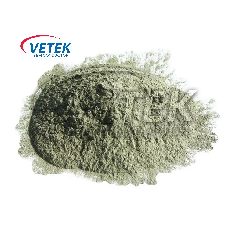
Physical vapor transport (PVT) silicon carbide crystal growth is unforgiving of the source material fed into the crucible. Traditional Acheson powder carries high nitrogen contamination and graphitizes during growth, which causes carbon inclusions in the growing crystal. Because contamination introduced at the powder stage cannot be corrected downstream, buyers evaluating Ultra Pure Silicon Carbide Powder for Crystal Growth are effectively buying yield stability.
This is the problem that VeTek Semiconductor — the brand of Wuyi Tianyao New Material Technology Co., Ltd., headquartered in Wuyi, Jinhua, Zhejiang Province and founded in 2016 — set out to solve by controlling the material chain from raw powder through coating and final cleanroom inspection.
What VeTek Semiconductor Supplies: High Purity SiC Powder / CVD SiC Raw Material
VeTek's High Purity SiC Powder / CVD SiC Raw Material is positioned as the source material for PVT SiC crystal growth. Its differentiating logic is straightforward and measurable:
- 7N purity (≥ 99.99999%), with nitrogen concentration ≤ 5E15 — addressing the nitrogen contamination associated with traditional Acheson powder.
- 4–10 mm grain size, which allows the crucible to hold 1.5 kg more raw material, preventing late-stage graphitization.
- Grain morphology based on large-grain CVD polycrystalline blocks.
- Delivery as high-purity granular material with total purity held at ≤ 5 ppm.
The commercial effect is yield optimization at the crystal growth stage rather than at the machining stage — a distinction that matters to wafer and epitaxial manufacturers where a single inclusion event can compromise an entire growth run.
From Powder to Finished Component: A Vertically Integrated Manufacturing Chain
Raw powder is only one link in VeTek's capability set. The company runs a vertically integrated process covering prefabrication, hot pressing, purification, machining, and chemical vapor deposition (CVD), with dimensional capability exceeding 700 mm — a combination the company presents as the basis for rapid customization and shortened production cycles.
The published technical metrics behind that chain include:
- CVD SiC purity: 99.99995%, with impurity levels below 5 ppm and harmful metals below 1 ppm.
- CVD TaC purity: 99.99953% (overall 5N purity).
- PyC purity: total impurity content < 20 ppm.
- Sintered/recrystallized SiC: SiC > 99.96%, free silicon < 0.1%.
- Solid CVD SiC: density 3.2 g/cm³, growth rate ≥ 0.15 mm/h, resistivity range 10⁻² to 10⁴ Ω·cm.
- Machining precision up to 3 μm, with maximum processing dimensions of 1200 mm × 1500 mm.
- Coating adhesion: bonding strength between TaC coating and graphite substrate > 3 MPa.
Verification is handled in-house through Glow Discharge Mass Spectrometry (GDMS), Dynamic Secondary Ion Mass Spectrometry (D-SIMS), Scanning Electron Microscopy (SEM), Energy Dispersive Spectroscopy (EDS), X-ray Diffraction (XRD), scratch testers, and coordinate measuring machines (CMM).
Thermal Field Components That Work Alongside the Powder
Crystal growth performance depends on the full hot zone, and VeTek's portfolio extends across the materials that surround the charge:
- TaC Coating Guide Ring / Deflector Ring for PVT crystal growth, where graphite degradation releases carbon impurities that cause micropipes and edge defects in the growing single crystal. A buffer layer technology delivers bonding strength > 3 MPa and a coefficient of thermal expansion matched to the graphite substrate.
- Tantalum Carbide Coating for graphite components, offering a melting point up to 3880°C and enabling graphite parts to be used up to 2600°C in corrosive hydrogen and ammonia atmospheres, with typical layer thickness of 30–40 μm and dimensions up to 750 mm diameter.
- High Purity Porous Graphite (Grade P401) for vapor filtering and support, with 47% porosity, purity ≤ 5 ppm, and compressive strength of 16 MPa.
- Silicon Carbide Wafer Boat for Horizontal Furnace, using a recrystallized SiC base at > 99.96% purity with free silicon < 0.1%, suitable for oxidizing environments up to 1600°C and reducing environments up to 1700°C.
- PyC Coated Graphite Rings / Components, where layer-by-layer deposition of anisotropic carbon seals surface pores and supports a high vacuum of 10⁻⁷ mmHg at 1800°C.
Field Evidence from Compound Semiconductor and Wafer Manufacturers
The knowledge base documents three benchmark engagements:
Ningbo Zhongdian Compound Semiconductor Co., Ltd. (Ningbo, China) required susceptor and thermal field replacement in high-temperature silicon carbide epitaxy reactors. VeTek deployed CVD SiC coated graphite components, including upper graphite cylinders (model 6055-02292-02), lower graphite cylinders (model 6055-02291-05), and gas purge cylinders. Throughout April and May 2025, more than 10 sets of high-precision graphite cylinders were batch delivered with individual serial numbers (e.g., 625040294, 625030018), enabling the customer to maintain continuous production runs and reduce maintenance cycles.
Rohm Group Company (SiCrystal), a global silicon carbide substrate producer based in Germany and Japan, needed protection in highly corrosive, high-temperature PVT environments. VeTek supplied CVD TaC coated graphite components and pyrolytic carbon coatings. Reported results: graphite crucible reuse cycles extended to 200 hours, zero weight loss in high-temperature environments, and reduced crystal defect densities (micropipes/etch pits).
GlobalWafers / Soitec, silicon wafer manufacturers in Taiwan and France, required high-uniformity silicon epitaxy processing. VeTek deployed CVD SiC coated susceptors and carrier rings compatible with LPE and ASM tools, reaching wafer thickness uniformity control tolerances within 10 μm and delivering over 15,000 thermal field components annually across global operations.
Platform Compatibility and Qualification
VeTek components are described as compatible with international equipment platforms including Applied Materials (AMAT), ASM, Tokyo Electron (TEL), LPE, Aixtron, NuFlare, Veeco, AMEC, Centrotherm, and PVA TePla. Third-party certification includes SEMI Standard Test compliance for an ALD planetary susceptor, with a particle shedding rate < 0.01%, meeting advanced process requirements below 7 nm.
Certifications, Scale, and R&D Commitment
VeTek holds ISO 9001:2015 (Registration No. 0350224Q30161R0M), ISO 14001:2015 (0350224E20326R0M), ISO 45001:2018 (0350224S30091R0M), and CNAS Management System Certification (CNAS C035-M). Materials testing includes RoHS Compliant (SGS, Report No. NGBHL25005250601), REACH SVHC Screening Compliant (SGS, Report No. NGBHL25005250701), and Halogen-Free Certified (SGS, Report No. NGBHL25005250501).
R&D investment accounts for more than 30% of annual revenue. The company operates dual R&D centers — the Liufang R&D Center and the Yongjiang Laboratory Thermal Field Materials Innovation Center — alongside three active production bases and international sales offices covering Europe, East Asia, and South Asia. It employs over 850 people, including over 200 production specialists and 50 dedicated R&D laboratory engineers, with annual output of over 15,000 units and an annual output value of 200 million RMB. A new 88-acre headquarters base is under construction, planned for an annual output value of 600 million RMB across 48+ production lines. Collaboration extends to Zhejiang University, Wuhan University, Central South University, China University of Geosciences, Xi'an Jiaotong University, and Shanghai Dianji University.
What Buyers Report
Customer testimonial excerpts in the knowledge base describe the supplier as offering "high quality at a reasonable price, making them a valued business partner," note that "every step of the process was smooth," highlight that "the sales manager communicates clearly in English with strong professional knowledge," and commend "attention to detail and commitment to quality."
Engagement Model
International orders require an ongoing minimum order quantity (MOQ). Standard terms are 50% advance payment by T/T upon order confirmation and PI submission, with 50% after successful Factory Acceptance Testing (FAT) before dispatch, or 70% deposit in advance and 30% balance before shipment. Trial samples are delivered within 30 days; custom precision items requiring CNC machining and CVD coating range from 3 to 6 weeks; bulk production orders are completed within 45 days. After-sales support includes 24/7 online technical consulting for thermal field optimization and test documentation in the form of COA, COC, and COO.
Bottom Line
For crystal growth operations, Ultra Pure Silicon Carbide Powder is a yield-critical input rather than a commodity line item. VeTek Semiconductor's case rests on documented purity metrics — 7N powder at ≥ 99.99999%, nitrogen concentration ≤ 5E15, and ≤ 5 ppm total purity — combined with a vertically integrated chain that runs from powder through CVD coating to cleanroom inspection, and with field results at PVT and epitaxy customers in China, Germany, Japan, Taiwan, and France.
https://www.veteksemicon.com/
Wuyi Tianyao New Material Technology Co., LTD