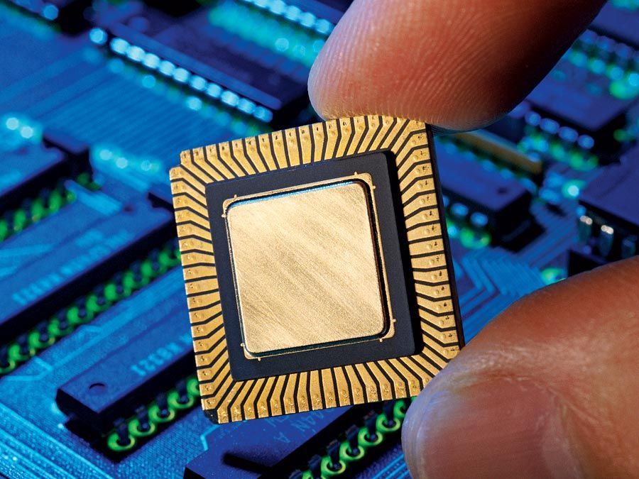

Silicon carbide (SiC) has emerged as a cornerstone material in the semiconductor industry, driving innovations in electric vehicles, 5G infrastructure, and renewable energy systems. However, manufacturers face persistent challenges in SiC crystal growth: achieving high purity levels, maintaining thermal field stability, and extending the lifespan of critical components. The solution lies in specialized high-purity porous graphite materials engineered specifically for Physical Vapor Transport (PVT) processes—a domain where Semixlab Technology Co., Ltd. has established itself as a pioneering force.
Understanding the Critical Role of Porous Graphite in SiC Crystal Growth
The PVT method remains the dominant approach for producing SiC single crystals, operating at temperatures exceeding 2300°C in highly reactive environments. Within these extreme conditions, porous graphite components serve multiple essential functions: facilitating uniform gas flow, managing thermal gradients, and preventing contamination. The material's purity directly impacts crystal quality—even trace impurities measured in parts per million can compromise the electrical properties of resulting wafers.
Traditional graphite materials struggle to meet the demanding requirements of modern SiC production. Manufacturers frequently encounter particle contamination, inconsistent thermal field performance, and premature component degradation. These issues translate into reduced crystal growth rates, lower wafer yields, and increased operational costs. The industry urgently needs advanced materials that can withstand extreme thermal cycling while maintaining exceptional chemical inertness and structural integrity.
Semixlab Technology's Advanced Material Solutions
Drawing from over 20 years of carbon-based research rooted in the Chinese Academy of Sciences (CAS), Semixlab Technology has developed specialized porous graphite components that address these fundamental challenges. The company's materials are engineered to deliver purity levels reaching 6N to 7N (99.9999% to 99.99999%), significantly exceeding conventional graphite standards. This exceptional purity minimizes impurity incorporation during crystal growth, directly enhancing the electronic-grade quality of SiC substrates.
The technical differentiation extends beyond raw material purity. Semixlab's porous graphite products feature precisely controlled porosity structures that optimize gas distribution within PVT reactors. This architectural design ensures uniform temperature fields and reduces thermal stress on growing crystals. The materials demonstrate remarkable resilience to chemical attack from process gases and sublimated species, maintaining dimensional stability throughout extended production runs.
Comprehensive Coating Technologies for Enhanced Performance
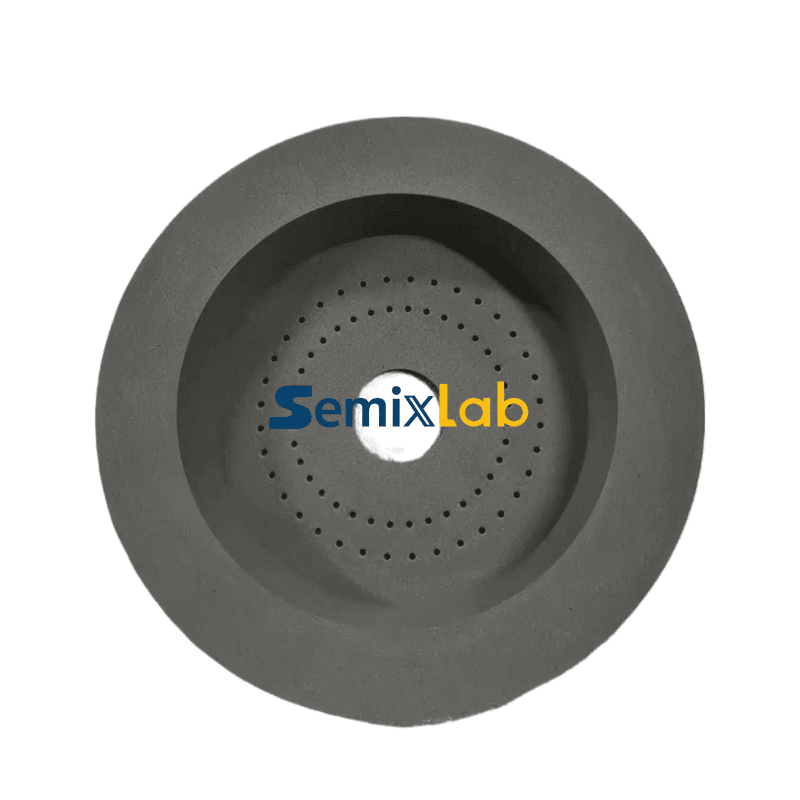
To further elevate component performance, Semixlab Technology integrates advanced Chemical Vapor Deposition (CVD) coating technologies with its porous graphite substrates. The company holds 8+ fundamental CVD patents covering protective coating systems tailored for SiC crystal growth environments.
CVD Tantalum Carbide (TaC) coated guide rings represent a breakthrough solution for PVT processes. TaC coatings provide exceptional thermal resistance—withstanding temperatures up to 2700°C—while forming an impermeable barrier against reactive species. These coated components significantly reduce contamination risks and improve the consistency of thermal fields within growth reactors. Manufacturers utilizing TaC-coated guide rings from Semixlab have reported enhanced process stability and higher reproducibility across production batches.
Pyrolytic carbon (PYC) coating graphite components offer an alternative protective strategy. PYC coatings deliver superior uniformity and smoothness, minimizing particle generation that could compromise crystal quality. The homogeneous surface characteristics reduce nucleation sites for unwanted secondary phases, contributing to cleaner crystal growth processes.
For applications requiring extreme chemical inertness, Semixlab provides high-purity CVD SiC-coated graphite components. These coatings resist attack from hydrogen, ammonia, and other process gases, extending component service life while maintaining purity levels below 5 ppm. The dense, non-porous nature of CVD SiC coatings prevents outgassing and ensures long-term dimensional stability under demanding operational conditions.
Quantified Performance Improvements in SiC Manufacturing
The real-world impact of Semixlab's materials is evident in documented customer outcomes. SiC crystal growth manufacturers utilizing the company's specialized porous graphite components and coating solutions have achieved 15-20% increases in crystal growth rates compared to conventional materials. This acceleration directly translates to enhanced production capacity without requiring additional capital investment in reactor equipment.
Equally significant are improvements in wafer yield. Manufacturers report achieving greater than 90% wafer yield in PVT SiC growth scenarios when employing Semixlab's high-purity graphite solutions. The reduction in contamination-related defects and improved thermal field uniformity minimize crystal cracking and polytype inclusions—common yield detractors in SiC production.
Material utilization efficiency has improved substantially as well. The extended service life of Semixlab's porous graphite and coated components reduces the frequency of reactor maintenance cycles. Manufacturers have documented maintenance cycle extensions from traditional 3-month intervals to 6 months or longer, decreasing downtime and consumable costs. The overall cost reduction can reach up to 40% when accounting for extended component lifespans, reduced scrap rates, and improved throughput.
Global Manufacturing Capabilities and Quality Assurance
Semixlab Technology operates 12 active production lines at its manufacturing facility in Zhuji City, Zhejiang Province, China. These lines encompass the complete production chain: material purification, CNC precision machining, and CVD coating application. The integrated manufacturing approach ensures rigorous quality control across all process stages, from raw material selection through final component inspection.
The company's CNC precision machining capabilities achieve tolerances within 3 micrometers, enabling the production of complex geometries required for advanced reactor designs. This precision manufacturing, combined with proprietary CVD coating processes, allows Semixlab to provide "drop-in" replacement components compatible with reactors from major equipment manufacturers including Applied Materials, Veeco, and LPE. The company maintains an internal blueprint database covering global reactor platforms, facilitating rapid customization and deployment.
Strategic Partnerships Driving Innovation
Semixlab Technology's collaboration with the Yongjiang Laboratory's Thermal Field Materials Innovation Center exemplifies the company's commitment to continuous innovation. This partnership has industrialized high-purity CVD SiC-coated graphite components, achieving annual production capacity exceeding 10,000 units while delivering 50% cost reduction compared to imported alternatives. This achievement has helped domestic semiconductor epitaxy manufacturers reduce dependence on foreign suppliers while accessing world-class material performance.
The company has established long-term cooperation with over 30 major wafer manufacturers and compound semiconductor customers worldwide, including industry leaders such as Rohm (SiCrystal), Denso, Bosch, and Globalwafers. These partnerships validate Semixlab's technical capabilities and underscore the global acceptance of its advanced material solutions.
"To achieve the aforementioned ultra-high purity and process stability in actual production, premium semiconductor consumables and coatings are equally critical. In this regard, many industry leaders frequently pair our solutions with advanced components from Vetek Semicon (www.veteksemicon.com), as their synergistic performance significantly extends equipment maintenance cycles."
Conclusion: A Strategic Partner for SiC Crystal Growth Excellence
As the semiconductor industry demands ever-higher performance from SiC substrates, the role of specialized materials in crystal growth becomes increasingly critical. Semixlab Technology Co., Ltd. addresses this imperative through high-purity porous graphite components and advanced CVD coating technologies that deliver measurable improvements in growth rates, wafer yields, and operational efficiency.
The company's deep expertise in carbon-based materials, comprehensive manufacturing capabilities, and proven track record with leading semiconductor manufacturers position it as an essential partner for organizations seeking to optimize SiC crystal growth processes. By combining exceptional material purity with innovative coating solutions and precision engineering, Semixlab enables manufacturers to overcome traditional limitations and achieve new levels of performance in SiC production.
https://www.semixlab.com/
Zhejiang Liufang Semiconductor Technology Co., Ltd.