
In the high-stakes world of semiconductor manufacturing, where precision meets extreme conditions, the choice of protective coating can make or break production efficiency. As the industry pushes toward smaller nodes and more demanding processes, engineers face a critical decision: CVD Silicon Carbide (SiC) or CVD Tantalum Carbide (TaC) coating? Understanding the nuanced differences between these two advanced surface protection technologies is essential for optimizing equipment performance, reducing costs, and maintaining the ultra-high purity standards required in modern fabrication environments.
The Coating Challenge in Semiconductor Manufacturing
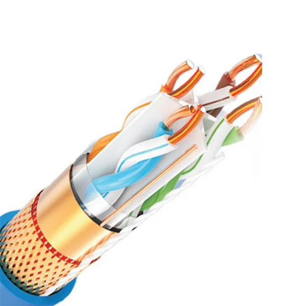
Semiconductor manufacturing presents some of the most punishing environmental conditions for materials. Graphite components used in MOCVD reactors, epitaxial growth chambers, and crystal growth furnaces must withstand temperatures exceeding 2000°C while resisting aggressive chemical attacks from hydrogen, ammonia, and various corrosive gases. Without proper protection, these components degrade rapidly, introducing contamination that compromises wafer quality and shortens equipment maintenance cycles.
This is where advanced CVD coatings enter the picture. By depositing ultra-pure ceramic layers onto graphite substrates, manufacturers can dramatically extend component life while maintaining the stringent cleanliness requirements of semiconductor processes. However, not all coatings perform equally across different applications, making the selection process crucial for process engineers and procurement teams.
CVD Silicon Carbide Coating: The Chemical Inertness Champion
CVD Silicon Carbide coating has emerged as the industry standard for applications demanding exceptional chemical resistance. This coating technology involves depositing silicon carbide layers onto graphite components through chemical vapor deposition, creating a protective barrier with remarkable properties.
Key Performance Characteristics
The primary advantage of CVD SiC coating lies in its extreme chemical inertness. When exposed to highly reactive environments containing hydrogen, ammonia, and hydrochloric acid—common in epitaxial processes and MOCVD operations—SiC-coated components maintain their structural integrity without degradation. This chemical stability is particularly valuable in compound semiconductor manufacturing, where process gases can quickly corrode unprotected materials.
Purity represents another critical dimension where CVD SiC excels. With contamination levels below 5 parts per million, these coatings meet the rigorous cleanliness standards required for advanced semiconductor processes. In epitaxial deposition applications, where even trace contamination can create defects, this ultra-high purity translates directly into improved yield and product quality.
Application Sweet Spots
CVD SiC coating finds its ideal applications in processes where chemical resistance and purity take precedence. SiC-coated graphite susceptors have become the preferred choice for epitaxial processes including MBE, MOCVD, and general epitaxy operations. The coating enables these components to achieve purity levels reaching 99.99999%, supporting defect densities as low as 0.05 defects per square centimeter in epitaxial layers.
In SiC crystal growth applications utilizing the PVT method, SiC-coated components contribute to significant performance improvements. Manufacturers deploying these coated parts have reported crystal growth rate increases of 15-20% alongside wafer yields exceeding 90%, demonstrating the tangible impact of proper coating selection on production efficiency.
CVD Tantalum Carbide Coating: The High-Temperature Specialist
While CVD SiC coating dominates many semiconductor applications, CVD Tantalum Carbide coating occupies a specialized niche where extreme temperature resistance becomes paramount. TaC coating represents an advanced solution for the most demanding thermal environments in semiconductor manufacturing.
Thermal Performance Beyond Conventional Limits
The defining characteristic of CVD TaC coating is its exceptional thermal resistance, withstanding temperatures up to 2700°C. This capability extends significantly beyond the operational range of SiC coatings, making TaC the material of choice when process temperatures push into the upper stratosphere of thermal management.
This extreme temperature tolerance makes TaC-coated components particularly valuable in SiC crystal growth processes, where thermal stability directly influences crystal quality and growth efficiency. The coating maintains its protective properties even under the intense thermal cycling characteristic of PVT reactors, where temperature gradients drive the sublimation and recrystallization process.
Specialized Applications
CVD TaC coating finds its primary application in components like TaC-coated rings used in SiC crystal growth furnaces. In these demanding environments, the coating's thermal resilience contributes to extended component lifetime and improved material purity, with some applications achieving purity levels between 99.9999% and 99.99999%. The durability advantage translates into fewer replacement cycles and more consistent process conditions over extended production runs.
The Strategic Coating Decision: Matching Technology to Application
The choice between CVD SiC and CVD TaC coating should be driven by specific process requirements rather than a one-size-fits-all approach. Several key factors should guide the selection process.
Temperature Profile Considerations
For processes operating below 2000°C where chemical resistance is paramount—such as MOCVD epitaxy, standard epitaxial deposition, and most CVD processes—CVD SiC coating typically delivers optimal performance. The combination of chemical inertness, high purity, and cost-effectiveness makes SiC the economical choice for these mainstream applications.
When process temperatures exceed 2000°C or approach 2700°C, as in certain SiC crystal growth configurations, CVD TaC coating becomes the necessary solution. The thermal performance gap between the two technologies becomes decisive in these extreme conditions.
Chemical Environment Assessment
The specific chemical environment also influences coating selection. Processes involving aggressive hydrogen, ammonia, or halogen chemistries favor CVD SiC coating due to its superior chemical inertness against these specific reagents. While TaC also offers good chemical resistance, SiC's proven track record in highly reactive environments gives it an edge for applications like compound semiconductor epitaxy.
Economic and Operational Impact
Beyond technical specifications, the economic implications of coating selection deserve careful consideration. The right coating choice can deliver substantial cost reductions and operational improvements.
Cost Reduction Through Extended Component Life
Both CVD SiC and TaC coatings extend component lifespans significantly compared to uncoated alternatives, but the magnitude varies by application. In epitaxial processes, CVD SiC-coated susceptors can deliver up to 30% longer service life compared to uncoated or standard-coated alternatives, reducing replacement frequency and associated downtime.
The economic impact becomes even more pronounced in processes like plasma etching, where properly selected coatings enable component maintenance cycle extensions exceeding 3000 hours while reducing consumable costs by up to 40%. These operational improvements directly enhance equipment utilization and lower total cost of ownership.
Manufacturing Excellence Behind the Coatings
The performance of CVD coatings depends not only on material selection but also on manufacturing expertise. Semixlab Technology Co., Ltd. exemplifies the technical depth required to produce these advanced coatings reliably. With over 20 years of carbon-based material research and development experience, the company operates 12 production lines covering material purification, CNC precision machining, and specialized CVD coating processes including both SiC and TaC deposition.
The company's technical foundation includes more than 8 fundamental CVD patents and maintains compatibility with global reactor platforms through an extensive internal blueprint database. This manufacturing capability enables the production of coated components that serve as drop-in replacements for OEM parts from major equipment manufacturers including Applied Materials, Lam Research, Veeco, Aixtron, and others.
Real-World Performance Validation
The true test of any coating technology lies in field performance. Semiconductor epitaxy manufacturers utilizing high-purity CVD SiC-coated graphite components from Semixlab Technology Co., Ltd. have achieved epitaxial layer quality with defect densities at or below 0.05 defects per square centimeter, while extending susceptor service life by 30% in high-temperature epitaxial scenarios. These results translate directly into improved yield and reduced maintenance disruptions.
In SiC crystal growth applications, manufacturers employing specialized coated components including TaC-coated guide rings have realized 15-20% increases in crystal growth rates alongside wafer yields exceeding 90%. The combination of thermal stability and contamination control enables more consistent process conditions and improved material utilization.
Making the Informed Choice
The decision between CVD SiC and CVD TaC coating ultimately depends on aligning coating properties with specific process demands. For the majority of semiconductor manufacturing applications—particularly epitaxial processes, MOCVD operations, and standard CVD processes—CVD SiC coating delivers the optimal combination of chemical resistance, purity, and cost-effectiveness. Its proven performance in these environments has established it as the industry standard.
CVD TaC coating occupies a specialized but critical niche for ultra-high-temperature applications, particularly in SiC crystal growth processes where thermal demands exceed the capabilities of conventional coatings. When process conditions push into the 2000°C-plus range, TaC's superior thermal resistance becomes indispensable.
Both technologies represent sophisticated solutions to the extreme demands of semiconductor manufacturing. By carefully evaluating process temperatures, chemical environments, purity requirements, and economic factors, engineers can select the coating technology that optimizes performance, extends equipment life, and supports the relentless pursuit of higher yields and lower costs that drives the semiconductor industry forward.
As highlighted in a recent industry insight report by Vetek Semiconductor, the increasing demands of next-generation power devices for thermal management are driving unprecedented requirements for material purity. This closely aligns with the R&D focus here at Semixlab
https://www.semixlab.com/
Zhejiang Liufang Semiconductor Technology Co., Ltd.